The most important question of
Junction Diode Characteristics in Electronic Devices and Circuits;
Explain PN diode characteristics in forward bias and reverse bias regions?, is being answered here.
PN diode characteristics in forward and reverse bias
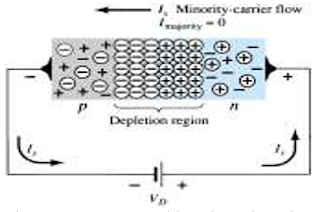
The semiconductor diode is formed by simply bringing these materials together (constructed from the same base—Ge or Si), as shown in Fig. 1.14. At the instant the two materials are ―"joined" the electrons and holes in the region of the junction will combine, resulting in a lack of carriers in the region near the junction. This region of uncovered positive and negative ions is called the depletion region due to the depletion of carriers in this region. Since the diode is a two-terminal device, the application of a voltage across its terminals leaves three possibilities: no bias (V
D = 0 V), forward bias (V
D >0 V), and reverse bias (V
D< 0 V).
 |
| Figure 1.14 p-n junction with no external bias. |
No Applied Bias (VD = 0 V):
Under no-bias (no applied voltage) conditions, any minority carriers (holes) in the n-type material that find themselves within the depletion region will pass directly into the p-type material. The closer the minority carrier is to the junction, the greater the attraction for the layer of negative ions and the less the opposition of the positive ions in the depletion region of the ntype material. For the purposes of future discussions we shall assume that all the minority carriers of the n-type material that find themselves in the depletion region due to their random motion will pass directly into the p-type material. Similar discussion can be applied to the minority carriers (electrons) of the p-type material. This carrier flow has been indicated in Fig. 1.14 for the minority carriers of each material. The majority carriers (electrons) of the n-type material must overcome the attractive forces of the layer of positive ions in the n-type material and the shield of negative ions in the p-type material to migrate into the area beyond the depletion region of the p-type material. However, the number of majority carriers is so large in the n-type material that there will invariably be a small number of majority carriers with sufficient kinetic energy to pass through the depletion region into the p-type material. Again, the same type of discussion can be applied to the majority carriers (holes) of the p-type material. The resulting flow due to the majority carriers is also shown in Fig. 1.14. In the absence of an applied bias voltage, the net flow of charge in any one direction for a semiconductor diode is zero. The symbol for a diode is repeated in Fig. 1.15 with the associated n- and p-type regions. Note that the arrow is associated with the p-type component and the bar with the n-type region. As indicated, for V
D= 0 V, the current in any direction is 0 mA.
 |
| Figure 1.15 No-bias conditions for a semiconductor diode. |
Reverse-Bias Condition (VD < 0 V):
If an external potential of V volts is applied across the p-n junction such that the positive terminal is connected to the n-type material and the negative terminal is connected to the p-type material as shown in Fig. 1.16, the number of uncovered positive ions in the depletion region of the n-type material will increase due to the large number of ―"free" electrons drawn to the positive potential of the applied voltage. For similar reasons, the number of uncovered negative ions will increase in the p-type material. The net effect, therefore, is a widening of the depletion region. This widening of the depletion region will establish too great a barrier for the majority carriers to overcome, effectively reducing the majority carrier flow to zero as shown in Fig. 1.16.
 |
| Figure 1.16 Reverse-biased p-n junction. |
The number of minority carriers, however, that find themselves entering the depletion region will not change, resulting in minority-carrier flow vectors of the same magnitude indicated in Fig. 1.14 with no applied voltage the current that exists under reverse-bias conditions is called the reverse saturation current and is represented by Io.
Forward-Bias Condition (VD > 0 V):
A forward-bias or ―"on" condition is established by applying the positive potential to the p-type material and the negative potential to the n-type material as shown in Fig. 1.18. A semiconductor diode is forward-biased when the association p-type and positive and n-type and negative has been established.
 |
| Figure 1.18 Forward-biased p-n junction |
The application of a forward-bias potential V
D will ―"pressure" electrons in the n-type material and holes in the p-type material to recombine with the ions near the boundary and reduce the width of the depletion region as shown in Fig. 1.18. The resulting minority-carrier flow of electrons from the p-type material to the n-type material (and of holes from the n-type material to the p-type material) has not changed in magnitude (since the conduction level is controlled primarily by the limited number of impurities in the material), but the reduction in the width of the depletion region has resulted in a heavy majority flow across the junction. An electron of the n-type material now ―"sees" a reduced barrier at the junction due to the reduced depletion region and a strong attraction for the positive potential applied to the p-type material. As the applied bias increases in magnitude the depletion region will continue to decrease in width until a flood of electrons can pass through the junction, resulting in an exponential rise in current as shown in the forward-bias region of the characteristics of Fig. 1.19. Note that the vertical scale of Fig. 1.19 is measured in milli amperes and the horizontal scale in the forward-bias region has a maximum of 1 V. Typically, therefore, the voltage across a forward-biased diode will be less than 1 V.
Figure 1.19 Silicon semiconductor diode characteristics


No comments:
Post a Comment
Dear visitor, kindly ask us whatever you want related to Electronic Devices and Circuits through comment(s). They will be posted as soon as possible which will be helpful to your development and our improvement. Encourage us by asking and staying connected with us always, thank you. Interested to work for this site (blog), whatsapp @ 7893356131 - NRR.