The most important question of Semi Conductor Physics in Electronic Devices and Circuits; Explain about N-type material and P-type material?, is being answered here.
There are two extrinsic materials of immeasurable importance to semiconductor device fabrication: n-type and p-type.
There are two extrinsic materials of immeasurable importance to semiconductor device fabrication: n-type and p-type.
n-Type Material:
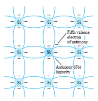
Both the n- and p-type materials are formed by adding a predetermined number of impurity atoms into a germanium or silicon base. The n-type is created by introducing those impurity elements that have five valence electrons (pentavalent), such as antimony, arsenic, and phosphorus. The effect of such impurity elements is indicated in Fig.1 (using antimony as the impurity in a silicon base). |
| Figure.1 Antimony impurity in n-type material. |
Note that the four covalent bonds are still present. There is, however, an additional fifth electron due to the impurity atom, which is unassociated with any particular covalent bond. This remaining electron, loosely bound to its parent (antimony) atom, is relatively free to move within the newly formed n-type material. Since the inserted impurity atom has donated a relatively ―free‖ electron to the structure: Diffused impurities with five valence electrons are called donor atoms. The effect of this doping process on the relative conductivity can best be described through the use of the energy-band diagram of Fig. 1.1.
 |
| Figure 1.1 Effect of donor impurities on the energy band structure. |
p-Type Material:
The p-type material is formed by doping a pure germanium or silicon crystal with impurity atoms having three valence electrons. The elements most frequently used for this purpose are boron, gallium, and indium. The effect of one of these elements, boron, on a base of silicon is indicated in Fig. 1.2. |
| Figure 1.11 Boron impurity in p-type material. |
Note that there is now an insufficient number of electrons to complete the covalent bonds of the newly formed lattice. The resulting vacancy is called a hole and is represented by a small circle or positive sign due to the absence of a negative charge. Since the resulting vacancy will readily accept a ―free‖ electron: The diffused impurities with three valence electrons are called acceptor atoms.
No comments:
Post a Comment
Dear visitor, kindly ask us whatever you want related to Electronic Devices and Circuits through comment(s). They will be posted as soon as possible which will be helpful to your development and our improvement. Encourage us by asking and staying connected with us always, thank you. Interested to work for this site (blog), whatsapp @ 7893356131 - NRR.